Analysis of Thin Film Solar Cell Design. Solar CELL
Abstract − Solar Cell is becoming the new
source of producing electricity. Light is converted into electricity in Solar
Cell. In our experiment we analyzed fill factor and conversion efficiency of a
solar cell. Our fill factor is 66.1582
and efficiency is 16.9166 %. There are ways these parameters can be
improved.
Keywords
− Solar Cell, Tcad, Conversion efficiency , Fill factor , Loss .
I. INTRODUCTION
Solar cell converts
optical signal into electrical signal. By this device , we can get electricity
without using any battery or voltage. So this is very important device for
rural areas where electricity is not available. And they don’t need to pay for
it. But in cloudy areas , less solar electricity is produced.
With increasing
population of the world, Engineers are finding it difficult to produce more
electricity and fulfill the necessity of electricity. So solar cell can be the
optimum solution of need of
electricity. It is economic and environment friendly energy with a very cheap cost.
In 1839 French
scientist Edmond Becquerel first discovered that light absorbed by a material
can produce electrical voltage.


Then years after years Selenium’s photoconductivity, first solar cell photoelectric effect, Silicon solar cell were discovered. Now, solar energy is used in space and more research is going on.[2].
Advantages of Solar Cells-Renewable energy - The energy can be used both to
generate electricity and heat in the house. Renewable energy is recovered from
the sun, the wind and waves - which in this case is the sun.Solar cells harness the energy
from the sun and transform this into usable electricity.
II. LOSSES IN SOLAR CELL
We get less current as
output than we expected. Because some losses occur and current decreases. The
losses can be of two types : Internal and external losses.
Internal losses consist
of Recombination and series or shunt loss .External losses consist of
reflection loss ,
transmission loss and
shadow loss. These losses are described below :
i)Reflection Loss :
When light falls on the surface of solar cell ,not all light goes through. Some
reflects and can’t pass through. This is called reflection loss.
ii)Transmission Loss :
All the light that goes into solar cell does not convert into electrical
signal. Rather some comes out from below. This is transmission loss. Amount
of this loss is little.
iii)Shadow Loss : Since
we place grid on top to collect current, light cannot pass through the grid and
there is a shadow below the grid. This is shadow loss.
iv)Recombination Loss :Sometimes
electron and proton recombines, so number of electron decreases , so current
decreases .This is called recombination loss.
v)Series and Shunt Loss
: When current flows , the losses occur in same way is series loss and parallel
way is shunt loss.
III. DEVICE STRUCTURE
We used a basic Solar
cell in our experiment. We took it from Silvaco website example 1[1] . Solar
cell are designed with some layers like TCO , buffer , Emitter , Absorber and
Al layer.
An ideal TCO is fully
transparent , has wide range of wave length, higher conductivity. For example: Graphene,
ITO, FTO. Buffer layer is the layer below TCO layer. In emitter layer p
diffusion is
used and in absorber layer n diffusion is used. We use p
above n , not n
above n , because when first p , then n is used , the
speed of electricity is more. At last Al layer is used so that Schottky
junction does not form. We use Al because work function of Al is greater than
4.1 eV.
IV. RESULT AND DISCUSSION
We analyzed the performance
parameter fill factor and conversion efficiency . We found out fill factor and
conversion efficiency by observing the following graphs.
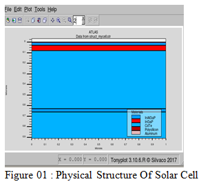
Figure 1 shows the physical
structure of solar cell used in our experiment.
Figure 02 : Cathode
current(A) vs Anode Voltage(V)
Figure 2 shows the
source photocurrent, available photo current
and cathode current with increase
of wavelength . The source photo current is linearly increasing with increase
of Anode voltage. But available photo current and cathode current decreases
when wavelength is greater than 0.87 nm which is wavelength of red light. So
red light and infra-red cannot be absorbed . So amount of current decreases.
Figure 03 : Anode
current / available photo curremt with respect to optical wavelength(µm) of Internal
and external quantum efficiency
Figure 3 represents how
much current we get with increase of wavelength. Current increases from 0.3 –
0.5 µm which is wavelength of Violet , ,Blue , Indigo. Current is nearly
constant from 0.5 – 0.8 µm which is
wavelength of green , yellow and orange. Current decreases in range 0.8 – 1 µm.
Because red and infrared light cannot be absorbed.
There are internal and
external losses in Solar Cell. Electrical losses occur in range of (0.3 – 0.5 )
µm and (0.8 - 1) . Electrical losses
consist of surface re-commendation , volume recombination and series and shunt
loss. Optical loss occurs in (0.5 – 0.8) µm. Optical loss consist of reflection
loss , transmission loss and shadow loss. These kinds of losses are described
in II. We can reduce the reflection loss by using anti-reflection coating
(ARC).
To find out the
efficiency and fill factor we need to observe the following curves.
Figure 04 : Anode power
vs Anode bias
Figure 4 represents
Anode power with respect to Anode bias. From this curve we get Maximum voltage
Vm. When power is maximum , we get maximum voltage. In this solar cell , Vm = 0.34
V when Pm = 0.0169229 W .
Figure 05 : Electric
field of Solar Cell.
In figure 5: This is
electric field of our solar cell. inside
a solar cell, the n-type
silicon's spare electrons jump over to fill the gaps in the p-type silicon.
This means that the n-type silicon becomes positively charged, and the p-type
silicon is negatively charged, creating an electric field across the cell.
Our Solar Cell is
n-type absorber base solar cell.
Figure 06 : Energy Band
Diagram of Solar Cell.
Electrons can gain enough energy to jump to the conduction band by
absorbing either a "phonon" (heat) or a "photon" (light)
with at least band gap energy. Photons with energy less than the band gap will
not separate electron pairs and simply pass through the solar cell.
Figure 07 : Fill Factor
of Solar Cell.
The Fill Factor (FF)
is essentially a measure of quality of the solar cell. It is calculated by comparing the maximum power to the
theoretical power (PT) that would be output at both the open circuit
voltage and short circuit current together
Dark current and photo current are shown. Dark
current is the current flowing opposite to photo current. We can get maximum
current from this curve when Vm = 0.34 V . We got maximum current Im = 0.0497732
A. We can get the efficiency from Tcad software.
Our efficiency was 16.9166
% .
We get Isc when V= 0 ,
Voc when I = 0 . From figure 7 . Using this value , we get fill factor by
following equation ,
F =
………. (1)
Our fill factor is 66.1582
which was good.
V.
CONCLUSION
Our Fill Factor was high. Our conversion efficiency was medium.
So design of our solar cell was not so much efficient. We need to improve it so
that conversion efficiency increases. We can do that by increasing doping of
top side or using materials of high bandgap on top layer and low bandgap on
bottom layer. Or using hetero junction i.e. different materials or using
materials having band gap of around 1.4 eV. We can also use multi junction to get a very good conversion efficiency.
VI.
REFERENCES


No comments